Expandable List
 Description:
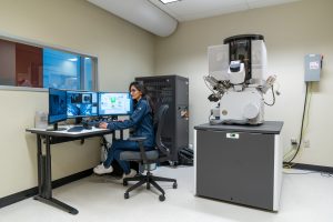
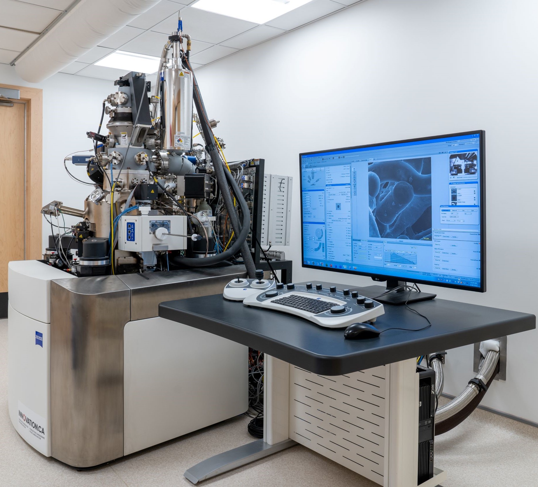
- The Helios 5 UC is a modern workhorse FIB targeted for typical FIB tasks such as cross-section analysis and sample preparation for TEM and APT.
Features:
- Assortment of detectors: ETD, TLD, ICE, MD, ICD, many with backscattered electron modes
- ThermoScientific Pathfinder EDS detector for EDS
- MultiChem gas-delivery system enables site-specific deposition of tungsten, platinum, and carbon
- Gas for selected carbon etching, Easy-lift for in-situ micromanipulation
- High-precision piezo-driven stage with Z-range of 10 mm and tilt range of -10 to 60 degrees
Contact: Sabaa Rashid for more information.
 Description:
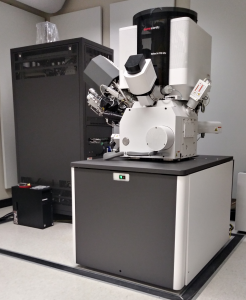
- The Helios 5 plasma focused ion beam (PFIB) provides the capacity to perform large area (up to 1 mm2) cross-sectioning, large 3D volume (up to 200 µm × 200 µm × 200 µm) characterization, and Ga+ free sample preparation by using an inductively coupled Xe+ plasma (ICP) source with an ion current that can reach as high as 2.5 µA.
Features:
- Oxford Instruments Ultim Max 100 electron-dispersive X-ray spectroscopy (EDS)
- Symmetry S2 electron backscatter diffraction (EBSD) detectors
Contact: Sabaa Rashid for more information.
Description:
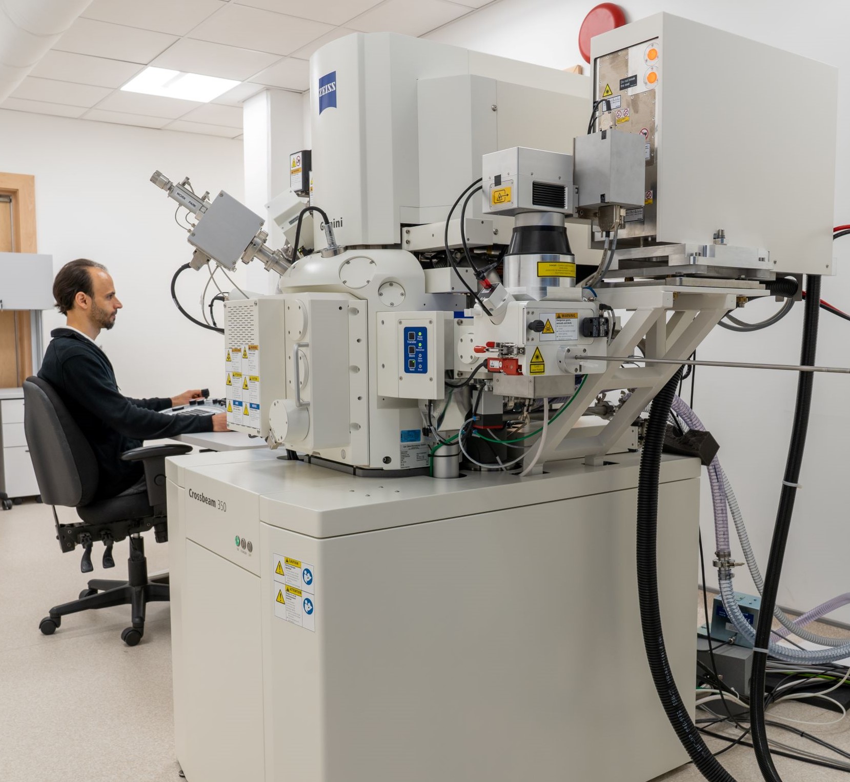 The Crossbeam 350 at CCEM is fully-equipped to handle a wide variety of scenarios, highlighted by a femtosecond laser that enables massive volumes of material ablation in addition to all the full functionality of a FIB-SEM.
Features:
- Femtosecond laser for massive volumes of material ablation
- SE2 and InLens secondary electron detectors
- In-column energy-selective backscattered (ESB) detector and retractable 4-quadrant annular backscattered electron detector
- Gas-injection systems enable site-specific deposition of tungsten or carbon
- Kleindiek MM3 micromanipulator with rotation for in-situ micromanipulation
- Large Z-range stage, tilt ranges from -4 to 70 degrees
- Leica cryo system with cold vacuum transfer capability
- Fibics scan generator with Atlas 5 software
- Correlation with 3D X-ray micro-CT data
Contact: Travis Casagrande for more information.
 Description:
- The Orion NanoFab is a dual beam instrument with two different FIB columns.
Features:
- Primary is a gas field ion source (GFIS) column which uses either He or Ne
- Second is a liquid metal ion source Ga column
- When imaging with He ions, the Orion can achieve up to 0.5 nm imaging resolution with a depth of field 5-10x that of a normal field emission SEM
- He ion beam capable of fine-scale milling and patterning (<10 nm)
- Ne beam offers improved milling rate with a trade-off on resolution, Ga FIB beam useful for high rate material removal
Applications:
- High resolution and high precision imaging, patterning, and advanced nanofabrication
Contact: Sabaa Rashid for more information.