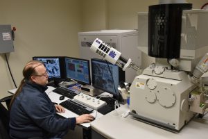
TEM
Expandable List
Description: 
- The TFS Spectra Ultra is an ultra-high-resolution, double-corrected HRTEM/STEM that operates at 30, 60, 200, and 300 keV.
Features:
- X-FEG source and an ultimono monochromator (10 meV at 60 kV)
- Ultra-X EDS detector
- Cs Probe and Image corrector (STEM resolution: 0.5 A at 300 kV / Information limit: 0.7 A)
- S-TWIN polepiece – constant thermal load, <15 min stabilization when switching kV’s
- HAADF + Panther STEM segmented detectors (DPC / iDPC)
- Tomography (Imaging/EDS)
- 4D-STEM using Ceta S Detector
- OptiSTEM+: automated corrector alignments
- OptiMono+: automated monochromator alignments
- Gatan ContinuumK3 GIF (EELS / EFTEM)
Applications:
- Well suited for high-energy-resolution analytical work down to single atoms.
Contact: Carmen Andrei for more information.
 Description:
- The Titan 80-300 LB is a high-resolution, image-corrected HRTEM/STEM that operates at 80 and 300 keV.
Features:
- High-brightness source and a monochromator
- Large-gap Cryo-Twin objective lens
- CEOS hexapole aberration corrector on the image-forming lens
- Gatan QuantumK2 GIF (0.8 eV resolution @300 kV)
- Single- and double-tilt holders, tomography holder, cryo-holder, heating holder
Applications:
- Suitable for high-energy-resolution analytical work including energy-filtered imaging
- Cryogenic capability and option to acquire and analyze electron tomography data
Contact: Carmen Andrei for more information.
 Description:
- The Thermo Scientific Talos 200X is an analytical TEM and STEM equipped with an X-FEG source and an adjustable high tension between 80 and 200 kV.
Features:
- Four in column SDD Super- X detectors for energy dispersive X-ray spectroscopy (EDS) signal detection
- CMOS detector for EELS acquisition with a measured energy resolution of 0.65 eV
- CETA 16M CMOS camera provides large area high framerate image acquisition capabilities
- HRTEM with a resolution of 0.1 nm and STEM with a resolution of 0.16 nm
- In-situ liquid and gas cell experiments
- Equipped with Protochips Axon software
Applications:
- Fastest and most precise EDS analysis in 2D and 3D
Contact: Carmen Andrei for more information.
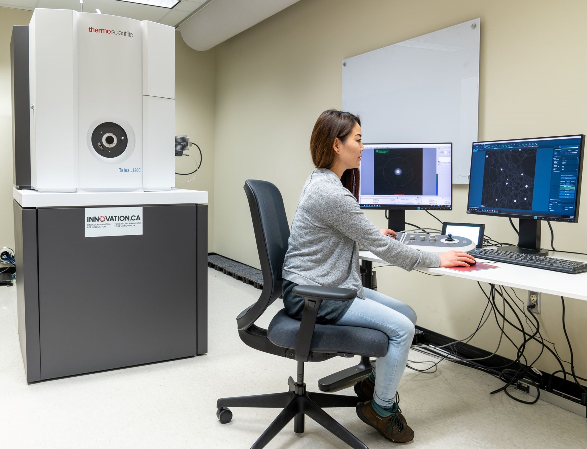 Description:
- The Thermo Scientific Talos L120C is a general purpose analytical TEM equipped with a LaB6 filament and an adjustable high tension between 20-120kV.
Features:
- Bruker XFlash 6TI30 EDS detector provides chemical mapping capabilities
- 4k CETA CMOS camera provides large area high framerate image acquisition capabilities
- Bright field or dark field TEM (information limit 0.36 nm @ 120kV), diffraction and scanning transmission electron microscopy (STEM)
Applications:
- Imaging of beam sensitive materials, metals and ceramics
- Primary training instrument for TEM at the facility
Contact: Carmen Andrei for more information.
 Description:
- The Nion HERMES 100 is a STEM instrument equipped with a probe corrector, monochromator and spectrometer that allows imaging and spectroscopy with both high spatial and ultra-high energy resolution.
Features:
- Operating voltages: 30keV, 60keV, 100keV
- Spatial resolution (sub 1 A at 60 KV)
- Energy resolution (sub 5 meV at 60 KV)
- Single- and double-tilt holders
Applications:
- Imaging specimens at atomic resolution
- Identifying features through imaging, diffraction, and spectroscopy
- Obtaining spatially resolved EELS maps
Contact: Brian Langelier for more information.
 Description:
- The JEOL 1200EX is a very user friendly TEM equipped with a tungsten filament and an adjustable high tension between 60-120kV.
Features:
- Quick grid exchange
- Pole piece design provides excellent contrast for biological samples
- Equipped with an AMT 4 megapixel digital camera
Applications:
- Suitable for imaging of beam sensitive materials and low dose imaging
Contact: Marcia Reid for more information.
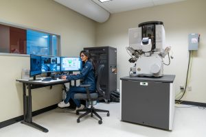
Scanning Electron Microscopes
Expandable List
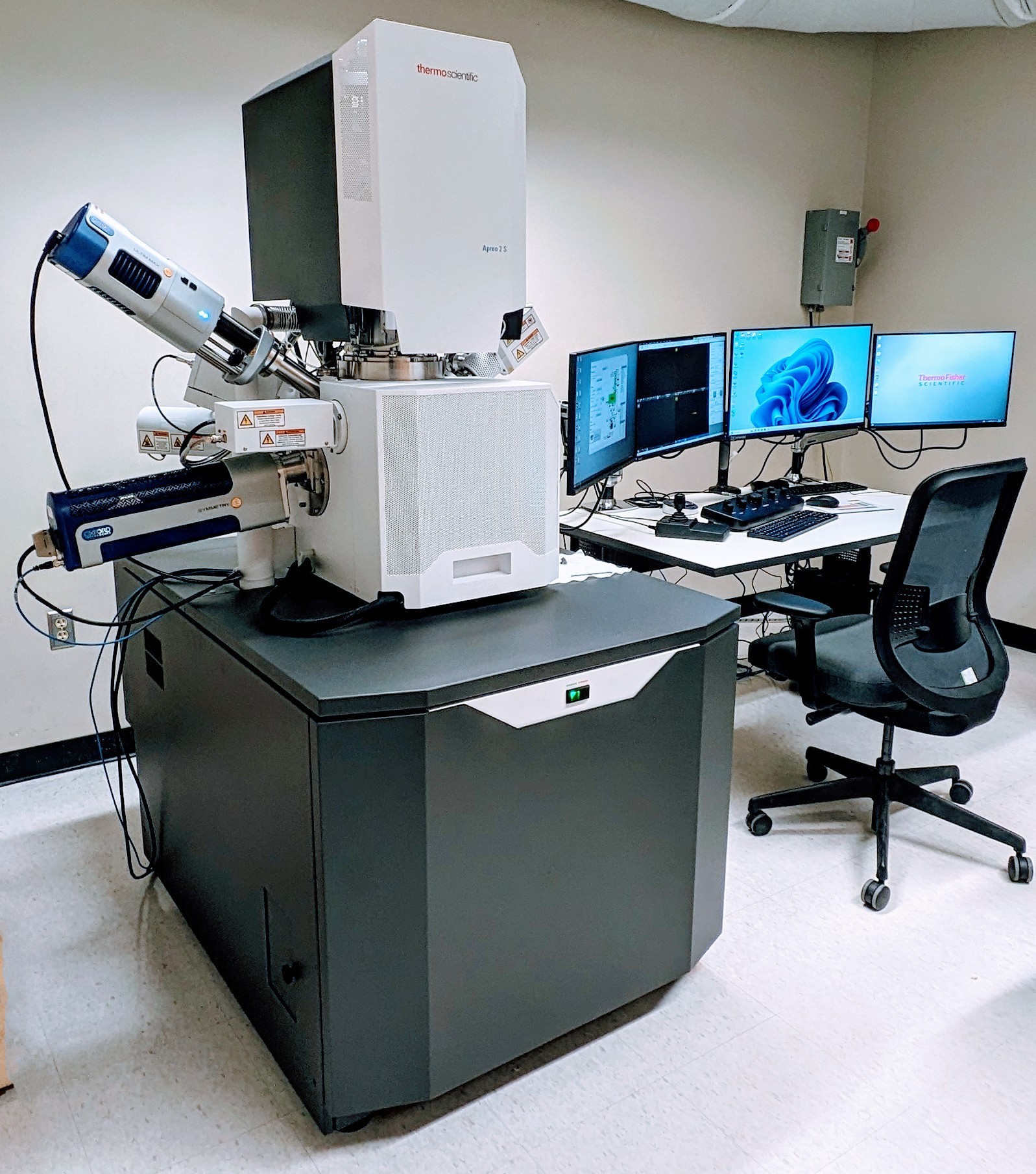 Description:
- The Apreo 2 S LoVac is a FEG-SEM with high resolution performance on a wide range of materials using both high and low vacuum.
Features:
- Standard Everhart Thornley electron detector along with a Trinity Detection System
- Operation modes include standard, Optiplan and immersion
- Equipped with drift compensated frame integration
- Beam deceleration can be used to enhance and modify imaging
- Electron channeling contrast imaging (ECCI) module
- Backscattered electron detector with CBS and ABS modes
- Oxford Instruments Ultimax 170 mm EDS
- Oxford Instrument Symmetry 3 EBSD
Applications:
- Collecting information on the sample composition, morphology, and surface features
- EBSD for electron crystallography
Contact: Chris Butcher for more information.
 Description:
- The FEI Magellan 400 is an extreme high-resolution SEM with sub-nanometer resolution.
- Operates at 1 to 30keV.
Features:
- In-situ plasma cleaner and a liquid nitrogen cold finger for analyzing highly labile and sensitive materials.
- SEM analysis of non-conductive materials at low beam energies.
- High collection efficiency in-lens detector and a unique low voltage, high contrast solid state detector.
- Two-mode objective lens with beam deceleration and immersion capabilities.
Applications:
- High surface sensitivity, high resolution, and enhanced contrast at low voltages.
Contact: Chris Butcher for more information.
 Description:
- The Thermo Scientific Quattro ESEM is an environmental SEM allowing for the study of materials in various conditions.
Features:
- Supports cooling and heating experiments in high vacuum and low vacuum.
- Chamber size allows for various in-situ experiments.
- Elemental information obtained with Thermo Scientific ChemiSEM Technology.
- Various detectors including ETD, low-vacuum SED (LVD), gaseous SED for ESEM mode (GSED), and IR camera.
- Live quantitative SEM image coloring based on energy-dispersive X-ray spectroscopy (EDS).
- Stage bias (beam deceleration): -4000 V to +50 V.
- Low vacuum mode: Up to 2600 Pa (H2O) or 4000 Pa (N2).
Applications:
- Imaging materials in a range of conditions.
- Elemental mapping with SEM software.
Contact: Jhoynner Martinez for more information.
 Description:
- The JEOL 6610LV is a tungsten filament equipped SEM with selectable low vacuum mode.
Features:
- Large chamber enabling observation of specimens up to 200mm in diameter.
- Resolution of 3.0nm at 30keV.
Applications:
- Viewing secondary electron and backscattered composition images simultaneously.
- EDS analysis.
Contact: Jhoynner Martinez for more information.
 Description:
- The TESCAN VEGA-II LSU SEM is a variable pressure SEM equipped with a tungsten filament.
Features:
- Conductive samples viewed via high vacuum mode, non-conductive samples under low vacuum conditions.
- Stage holds 7 stubs (13mm diameter) at one time and allows for 360-degree rotation and 50-degree tilt.
- Peltier cooling stage available.
- SE and BSE imaging done simultaneously.
- Equipped with an X-MAX 80mm2 EDS detector and INCA software.
Contact: Marcia Reid for more information.
Focused Ion Beam
Expandable List
 Description:
- The Helios 5 UC is a modern workhorse FIB targeted for typical FIB tasks such as cross-section analysis and sample preparation for TEM and APT.
Features:
- Assortment of detectors: ETD, TLD, ICE, MD, ICD, many with backscattered electron modes
- ThermoScientific Pathfinder EDS detector for EDS
- MultiChem gas-delivery system enables site-specific deposition of tungsten, platinum, and carbon
- Gas for selected carbon etching, Easy-lift for in-situ micromanipulation
- High-precision piezo-driven stage with Z-range of 10 mm and tilt range of -10 to 60 degrees
Contact: Sabaa Rashid for more information.
 Description:
- The Helios 5 plasma focused ion beam (PFIB) provides the capacity to perform large area (up to 1 mm2) cross-sectioning, large 3D volume (up to 200 µm × 200 µm × 200 µm) characterization, and Ga+ free sample preparation by using an inductively coupled Xe+ plasma (ICP) source with an ion current that can reach as high as 2.5 µA.
Features:
- Oxford Instruments Ultim Max 100 electron-dispersive X-ray spectroscopy (EDS)
- Symmetry S2 electron backscatter diffraction (EBSD) detectors
Contact: Sabaa Rashid for more information.
Description:
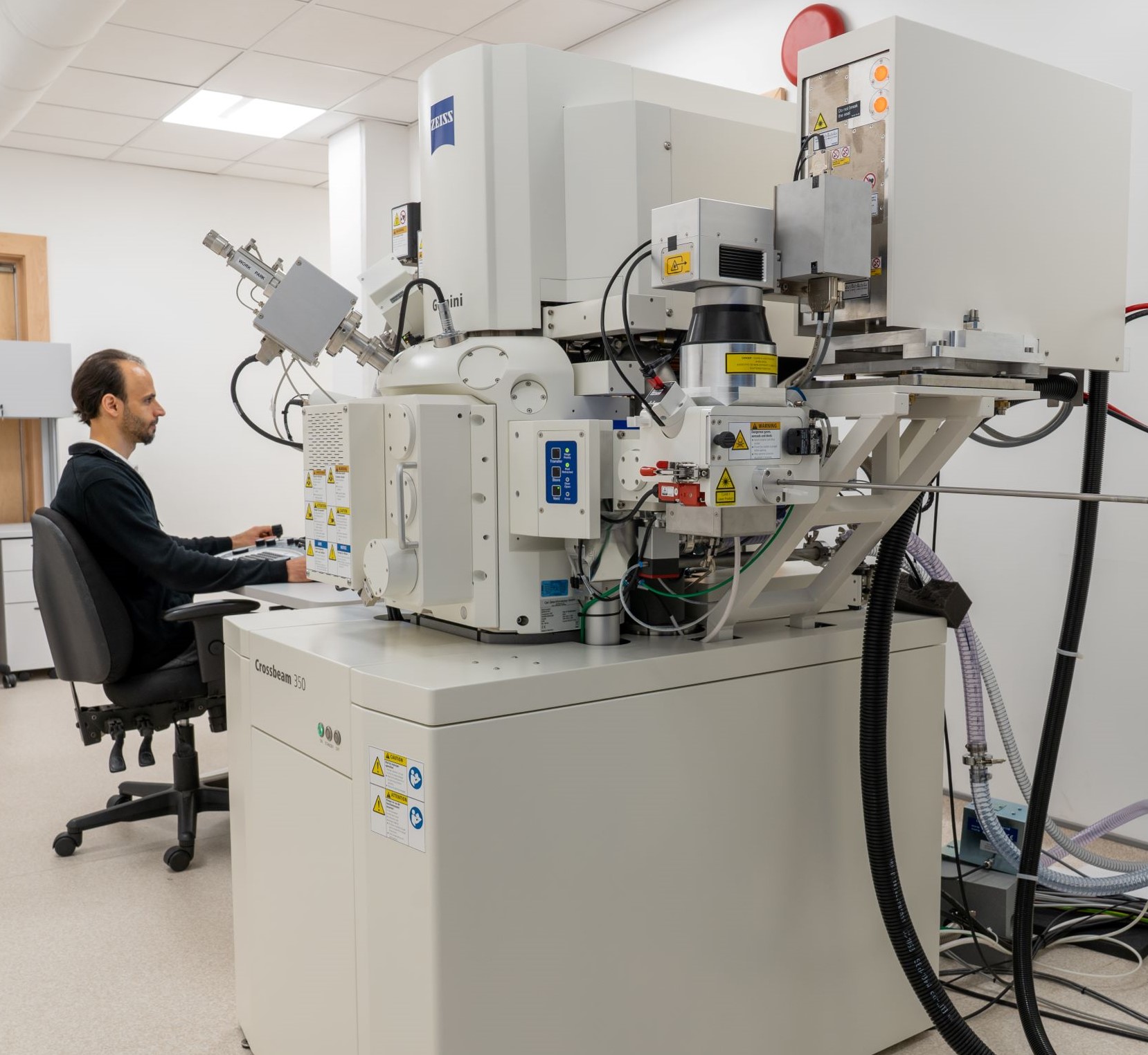 The Crossbeam 350 at CCEM is fully-equipped to handle a wide variety of scenarios, highlighted by a femtosecond laser that enables massive volumes of material ablation in addition to all the full functionality of a FIB-SEM.
Features:
- Femtosecond laser for massive volumes of material ablation
- SE2 and InLens secondary electron detectors
- In-column energy-selective backscattered (ESB) detector and retractable 4-quadrant annular backscattered electron detector
- Gas-injection systems enable site-specific deposition of tungsten or carbon
- Kleindiek MM3 micromanipulator with rotation for in-situ micromanipulation
- Large Z-range stage, tilt ranges from -4 to 70 degrees
- Leica cryo system with cold vacuum transfer capability
- Fibics scan generator with Atlas 5 software
- Correlation with 3D X-ray micro-CT data
Contact: Travis Casagrande for more information.
 Description:
- The Orion NanoFab is a dual beam instrument with two different FIB columns.
Features:
- Primary is a gas field ion source (GFIS) column which uses either He or Ne
- Second is a liquid metal ion source Ga column
- When imaging with He ions, the Orion can achieve up to 0.5 nm imaging resolution with a depth of field 5-10x that of a normal field emission SEM
- He ion beam capable of fine-scale milling and patterning (<10 nm)
- Ne beam offers improved milling rate with a trade-off on resolution, Ga FIB beam useful for high rate material removal
Applications:
- High resolution and high precision imaging, patterning, and advanced nanofabrication
Contact: Sabaa Rashid for more information.
Atom Probe Tomography
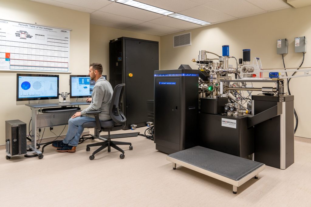
Cameca LEAP 5000 XS
Description:
- The Local Electrode Atom Probe (LEAP) 5000 XS from CAMECA Instruments Inc. is a high-resolution material analysis system that provides quantitative three-dimensional elemental and isotopic mapping with sub-nanometre resolution.
Features:
- Wide field-of-view and improved ion optics for high-quality spatial resolutions
- New detector technologies for unmatched multi-hit detection capabilities and detection efficiencies
- Laser capabilities using an ultraviolet laser (355 nm wavelength) for expanded material range
- Large range of pulse repetition rates for fast data acquisition times
- Vacuum and Cryo Transfer Module (VCTM) enables analysis of cryogenic and/or air sensitive materials
Field-evaporation of ions for material examination
- Reconstruction of collected data to yield a 3D computer model of the material
- Live-time mass-spectrum calibration and 3D data reconstruction for improved data quality
- Equipped with CAMECA AP Suite 6 software for easy and efficient data analysis
Applications:
- Characterization of dopants in semiconductors
- Analysis of alloying elements in steels
- Trace element segregation to interfaces and clusters
- Isotope ratio measurements in minerals
- Generation of 1D concentration profiles and 2D maps with atomic sensitivity
Contact: Gabe Arcuri for more information.
Auger Spectroscopy
JEOL JAMP-9500F FE-Auger
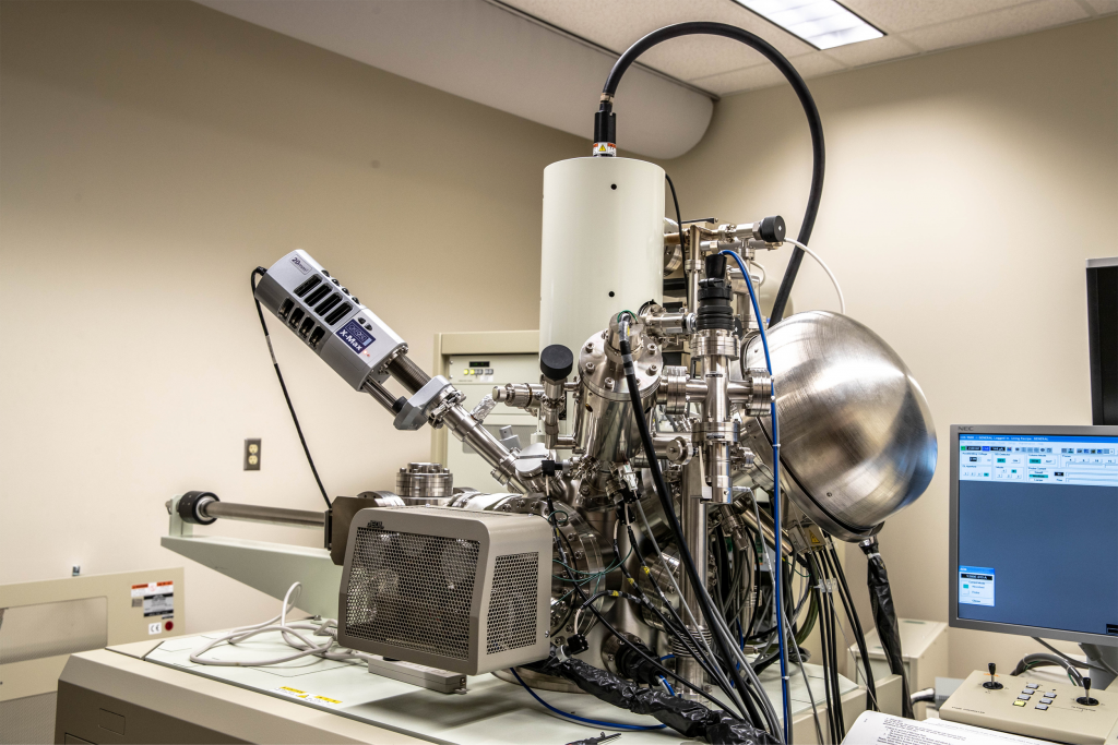
Description:
- The JEOL JAMP-9500F FE-Auger is a high-sensitivity instrument for surface analysis.
- It offers very high spatial resolution with a minimum probe diameter of 8nm and high energy resolution.
Features:
- Hemispherical electrostatic energy analyzer with a large acceptance angle
- Multi-channel detector for element detection with concentrations as low as 0.2 atomic%
- Incorporation of SEM for sample imaging
- EDXS detector for quick preview analysis and precise location selection
- In-situ ion gun for selective milling and depth profiling
- Detection of elements with concentrations as low as 0.2 atomic%
- Depth profiling to a depth of a few hundred nanometers
- Removal of contamination and neutralization of surface charging for non-conductive samples using the ion gun
Applications:
- Surface analysis with high sensitivity and spatial resolution
- Depth profiling for material characterization
- Contamination removal and surface charge neutralization for non-conductive samples
Contact: Travis Casagrande for more information.
X-ray CT
Expandable List
 Description:
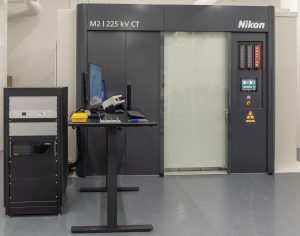
- The Nikon M2 225 KV CT is a high-performance X-ray computed tomography (CT) scanner with a maximum voltage of 225 kV and maximum power of 450 W.
- Features a tungsten target X-ray source bombarded with high-energy electrons.
- Provides fast and accurate 3D imaging of a wide range of materials, including metals, plastics, and composites, facilitating non-destructive testing, quality control, and materials research.
- Offers a large field of view and a high-resolution detector for detailed examination of internal structure.
Specifications:
- X-ray tube voltage: 50 – 225 kV
- Detector type: flat-panel
- Field of view: up to 300 mm in diameter and 500 mm in length
- Magnification: geometric
- Spatial resolution: up to 3 µm
Contact: Pardis Mohammadpour for more information.
 Description:
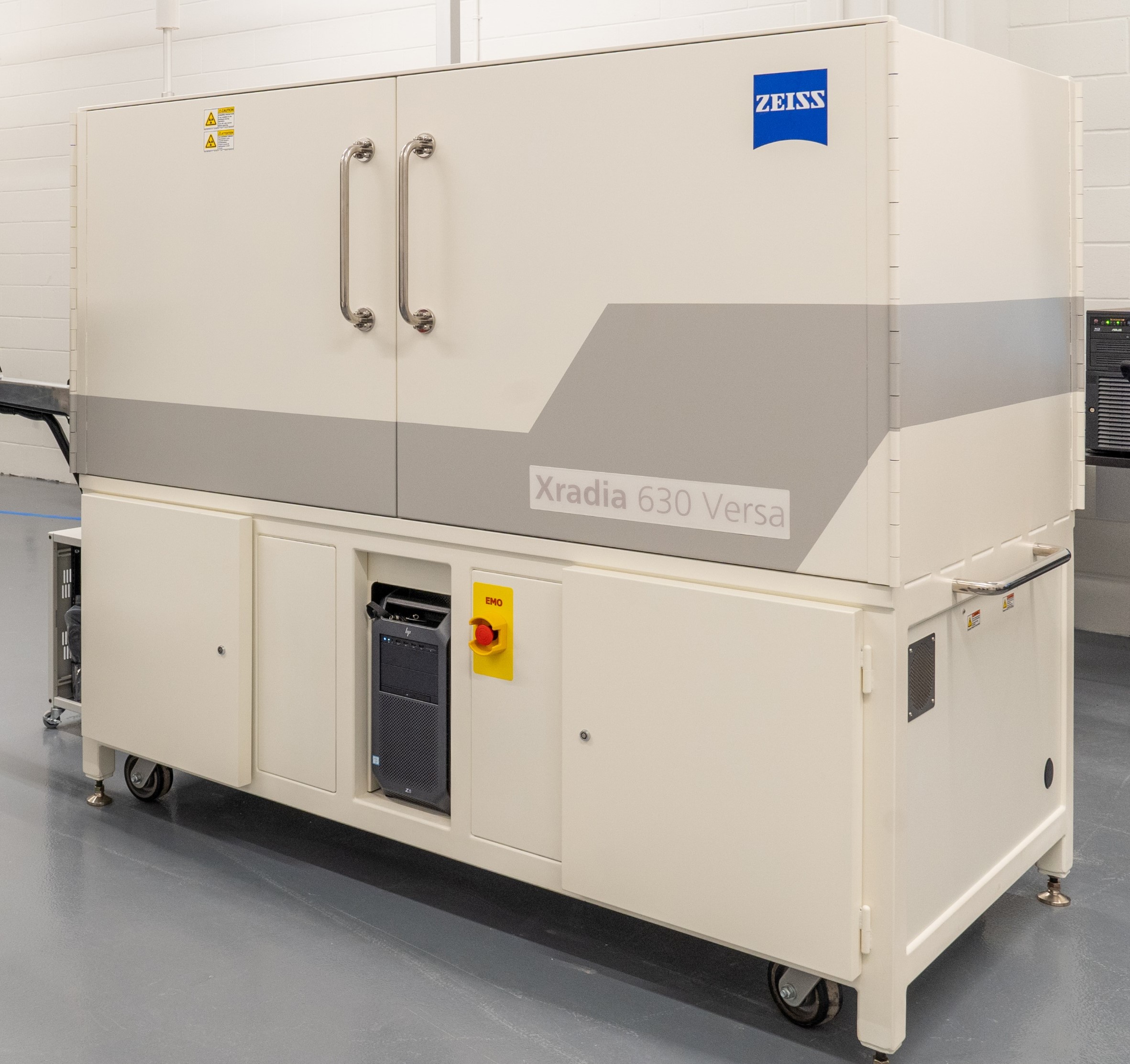
- The Zeiss Xradia 630 Versa is a high-resolution 3D X-ray microscope designed for non-destructive imaging of various sample types and length scales, ranging from sub-micron to millimeter ranges.
- Provides exceptional resolution performance (450 nm with maximum achievable voxel size of 40 nm) across an energy range of 30 kV to 160 kV, maximum 25 W.
- Equipped with dual-stage magnification feature using advanced synchrotron-caliber optics and RaaD™ (Resolution at a Distance) technology for high resolution even at large working distances.
- Enables 3D crystallographic data retrieval through Laboratory-based Diffraction Contrast Tomography (LabDCT), offering insight into microstructure, texture, and strain of materials.
- Utilizes AI-based reconstruction technology, ZEISS DeepRecon Pro, for faster throughput or higher quality images.
Specifications:
- X-ray tube voltage: 30 – 160 kV
- Detector type: flat-panel detector, objectives (0.4X, 4X, 20X, 40X-Prime)
- Maximum field of view: up to 140 mm in diameter, 93 mm (single) and 165 mm (stitched) in height
- Magnification: geometric, optical lens
- Spatial resolution: 450 nm with maximum achievable voxel size of 40 nm
- Maximum mass capacity: 25 kg
Contact: Pardis Mohammadpour for more information.